DEI3283-SMS
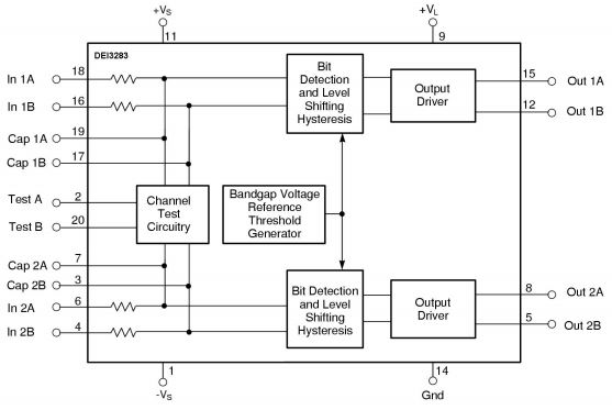
The DEI3283 consists of two analog ARINC 429 receivers which take differentially encoded ARINC level data and convert it to serial TTL level data. The DEI3283 provides two complete analog ARINC receivers with no external components required. Input level shifting thin film resistors and bipolar technology allow ARINC input voltage transients up to ±200 V without damage to the DEI3283. Each channel is identical, featuring symmetrical propagation delays for better high-speed performance. Input common mode rejection is excellent and threshold voltage is stable, independent of supply voltage. Data outputs are TTL and CMOS compatible. Two TTL compatible test inputs used to test the ARINC channels are available. They can be used to override the ARINC input data and set the channel outputs to a known state. The DEI ARINC line driver family IC’s are companion chips to the DEI3283 line receiver. Together they provide the analog functions needed for the ARINC 429 interface.
Features
- Two separate analog receiver channels
- Converts ARINC 429 levels to serial data
- ARINC 429 inputs withstand +/-200 V
- TTL inputs to test complete analog/digital RX function
- TTL and CMOS compatible outputs
- Low power dissipation
- Internal band gap voltage reference
- MIL-STD-883B burn-in screening available
- Package Options: 20 Lead ceramic DIP, 20 Terminal ceramic LCC, and 20 Lead SOIC
- Direct replacement for Fairchild/Raytheon RM3283 and RM3183 and Holt HI-8482
Attributes
Functional Description The DEI3283 contains two discrete ARINC 429 receiver channels. Each channel contains three main sections: an input signal conditioning network, a window comparator, and a logic output buffer stage. A test function is common to both channels. The input network comprises resistors and current switching circuits. It conditions the ARINC inputs with overvoltage protection, test signal injection, and biasing suitable for the comparators. The network provides excellent input common mode rejection. The window comparators detect ARINC pulse transitions in the signals from the input network. An ARINC input “High” state results in a logic 1 on OUT_A, and an ARINC input “Low” state results in a logic 1 on OUT_B. An ARINC input “Null” state forces both outputs to logic 0. Threshold and hysteresis voltages are generated by a band gap voltage reference to maintain stable switching characteristics over temperature and power supply variations. The logic output buffer stage generates TTL/CMOS compatible logic outputs. For built-in test capability, the TESTA/B inputs are provided to force the outputs to a predetermined state regardless of the ARINC input state. The test stimulus exercises the window comparators and logic output buffers; the ARINC input signals are not affected. If the test inputs are not used, they should be grounded.