DEI3182A-DMB
The DEI3182A is a complete differential line driver IC. When Data A = Data B or Sync or Clock Signal is low, the driver forces the output to a Voltage Null level (0V ± 250 mV). Designed to address the ARINC 429 Standard, the DEI3182A has output rise and fall times that can be adjusted by the selection of an external capacitor (CA or CB) and an output voltage range adjustable through an externally applied VREF signal. All logic inputs and sync control inputs are TTL/CMOS compatible. The device is constructed on a monolithic IC using a junction-isolated bipolar process. SiCr resistors in the internal bias circuitry provide for stable bias currents and a tighter tolerance of output impedance. The DEI3182A is available in 16-lead ceramic side-brazed DIP and can be ordered with MIL-STD-883B burn-in screening.
Features
- Adjustable rise and fall times
- Low supply current
- Capable of driving 30 nF || 400Ω
- Digitally selectable 12.5 or 100 kbit/sec data rate
- Adjustable output voltages swing
- Output over-voltage protected
- Short circuit tolerant
- TTL and CMOS compatible inputs
- MIL-STD-883B burn-in screening available
- Package Options:16L SB DIP, 16L CERDIP, 28L CLCC
- Direct replacement for Fairchild/Raytheon RM3182A
Attributes
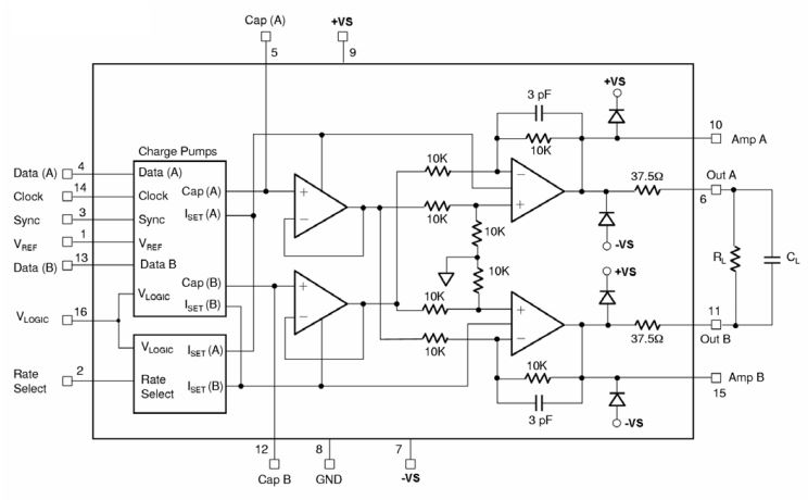
Functional Description The DEI3182A is a complete differential line driver IC. When Data A = Data B or Sync or Clock Signal is low, the driver forces the output to a Voltage Null level (0V ± 250 mV). Designed to address the ARINC 429 Standard, the DEI3182A has output rise and fall times that can be adjusted by the selection of an external capacitor (CA or CB) and an output voltage range adjustable through an externally applied VREF signal. All logic inputs and sync control inputs are TTL/CMOS compatible. The device is constructed on a monolithic IC using a junction-isolated bipolar process. SiCr resistors in the internal bias circuitry provide for stable bias currents and a tighter tolerance of output impedance. The DEI3182A is available in 16-lead ceramic side-brazed DIP and can be ordered with MIL-STD-883B burn-in screening. The device contains three main functional blocks. The first block is a digital section used to decode the ARINC Clock, Synchronization, and Data inputs as shown in Block Diagram. This block takes these inputs and channels the data to the charge pump circuits. The second functional block is a charge pump circuit that is used to control the output waveform and its timing characteristics. This is achieved through charging and discharging a capacitor with a known current. The capacitor is user selectable, and is connected between CA or CB pins and ground. A rate select pin (digital input) enables to set the rise and fall time. If this pin is tied to ground, the device functions in the high rate. This mode is recommended if the user does not have an application requiring data rate switching. In the table below, recommended capacitor values are given for each possible data combination. The last functional block of the device consists of a voltage follower and a high power output differential amplifier. The voltage follower buffers the signals presented at the charge caps and presents the mirrored signal to the difference amplifier to drive the ARINC line. Two different outputs are available from the differential amplifiers: Amp A, Amp B, and Out A, Out B. The outputs Amp A and Amp B are the direct outputs of the power amplifier. The outputs Out A and Out B include 37.5Ω series resistors added to minimize bus reflections by matching the power amplifier’s output impedance to the cable’s impedance of 75Ω . Amp A and Amp B may be used to customize the output impedance of the device. These outputs can also be used to enhance the device’s drive capability. For example, driving the standard 30 nF || 400Ω load defined in the ARINC specifications (see output drive capability and capacitive loads for more details). All outputs are protected from voltage spikes with diodes connected between the output pins and the supply lines.