DEI3093-QES-G
The DEI3093 is an ARINC 429 transceiver (2RX/1TX) CMOS integrated circuit. It provides the interface between an ARINC 429 avionics data bus and a Serial Peripheral Interface (SPI) enabled host such as a microcontroller or ASIC. The four SPI control/data signals are CMOS/TTL compatible. The IC operates from a single 3.3V power supply.
Features
- ARINC 429 Transceiver with SPI interface to host and single 3.3V supply
- TX includes:
- ARINC 429 Line Driver
- 32 word FIFO
- Dual RXs include:
- ARINC 429 Line Receiver with lighting protection
- 32 word FIFO
- Label filter for any label combination
- Three priority label registers
- 10 MHz Serial Peripheral Interface (SPI) for control/status and data IO
- On-chip DC/DC converter for ARINC 429 voltages
- Package:
- 44L QFN 7x7mm
- 44L PQFP 10 x10mm body
- Temperature range:
- -55 to +85°C
Attributes
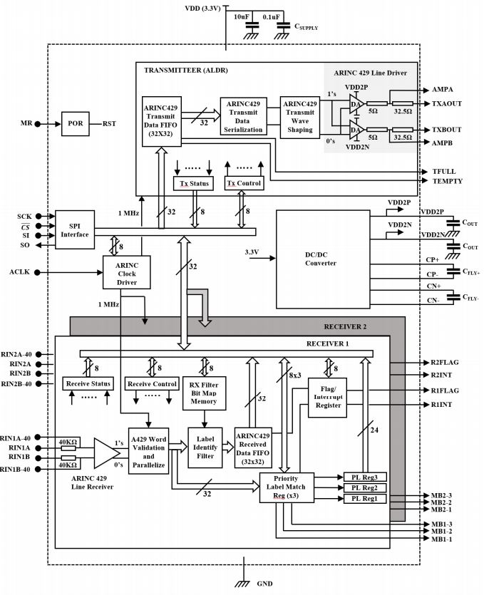
Functional Description The DEI3093 is an ARINC 429 transceiver (2RX/1TX) CMOS integrated circuit. It provides the interface between an ARINC 429 avionics data bus and a Serial Peripheral Interface (SPI) enabled host such as a microcontroller or ASIC. The four SPI control/data signals are CMOS/TTL compatible. The IC operates from a single 3.3V power supply. The ARINC 429 interface comprises two receivers and one transmitter. Each receiver offers user-programmable label recognition for up to 256 possible labels, a 32 x 32 Receive FIFO, three Priority Label quick-access single-buffered registers and an on-chip analog line receiver. The RX inputs in conjunction with external 40KΩ resistors are tolerant of DO160 Level 3 pin injection stress. Figure 1 shows a detailed block diagram of the device. The transmitter offers a 32 x 32 Transmit FIFO and built-in line driver. The line driver operates from a single 3.3V supply and includes an on-chip DC/DC converter to generate the voltage levels needed to drive the ARINC 429 bus directly. The output resistor options provide flexibility in applying TVS lighting protection of the line driver. The SPI interface provides access to the on-chip control/status and data registers. The control registers configure the application options of the transmitter, receivers, RX filters, RX priority registers, clock divider and the flag/interrupt outputs. Status registers indicate the state of the FIFOs (RX and TX) and RX priority registers. The RX and TX status may be monitored via programmable interrupt and status pins and/or by polling status registers via the SPI interface. Pins 1, 29, and 34 are non-connected (NC) pins.