DEI1148-QMS-G
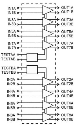
The DEI1148 is a BiCMOS device which contains eight differential line receivers. Each receiver channel translates incoming ARINC 429 data bus signals (tri-level RZ bipolar differential modulation) to a pair of TTL/CMOS logic outputs. Each channel operates independently and meets the requirements of the ARINC 429 Digital information Transfer Standard.
Features
- Octal ARINC 429 to TTL/CMOS logic line receivers
- Operates from single +5 V ± 10% or 3.3 V ± 10% power supply
- Operates in high noise environment
- Input Common Voltage Range: ± 20 V
- 2 V minimum Input hysteresis
- ARINC inputs internally protected to lightning requirements of DO-160 Level A3
- Withstands inadvertent short to 115 Vac on inputs
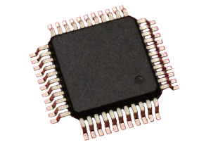
- Package: 44L MQFP, 13.9mm footprint
Attributes
Functional Description The DEI1148 is a BiCMOS device which contains eight differential line receivers. Each receiver channel translates incoming ARINC 429 data bus signals (tri-level RZ bipolar differential modulation) to a pair of TTL/CMOS logic outputs. Each channel operates independently and meets the requirements of the ARINC 429 Digital information Transfer Standard. The device is designed to operate in a high noise environment. Inputs are accepted over a ±20 V common mode voltage range and the receivers provide over 2 Volts of hysteresis. Circuit speed is optimized to reject high frequency transients. The DEI1148 device provides logic level TEST inputs for built in system test. There are two TEST input ports, each force the outputs of four receivers to the specified ZERO, ONE or NULL state. The ARINC inputs are ignored when the device is in test mode. The ARINC inputs incorporate on-chip lightning protection by use of high value resistors on the inputs to minimize IR heating. The resistors have dielectric isolation to withstand the voltage transients. The inputs withstand lightning induced transients up to and including DO160 Level 3 pin injection levels. Higher levels can be achieved with the addition of external TVS devices between the inputs and VSS, or alternately, TVS devices in combination with series current limiting resistors between the ARINC bus and the IC/TVS node. The series resistors reduce the power requirement and size of the TVS. Resistor values up to 10K ohms are feasible. The ARINC inputs withstand inadvertent short to 115 Vac aircraft power without sustaining damage.