DEI1038-G
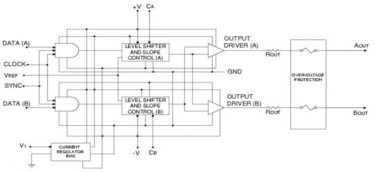
The ARINC 429 Line Driver Circuit is a bipolar monolithic IC designed to meet the requirements of several general aviation serial data bus standards. These include the differential bipolar RZ types such as ARINC 429, ARINC 571, and ARINC 575 as well as the differential NRZ types such as RS-422.
Features
- ARINC 429 Line Driver for high speed (100KHz) and low speed (12.5KHz) data rates.
- Pin Compatible with HI-8383J including 13Ω output resistor.
- Low EMI RS-422 Line Driver mode for data rates up to 100 KHz.
- Adjustable Slew rates via external capacitors.
- Inputs TTL and CMOS Compatible.
- Low Quiescent Power of 125mW (typical)
- Programmable output differential range via VREF pin.
- Outputs are not fused.
- Drives full ARINC load of 400Ω and 0.03µF.
- -55°C to +85°C operating temperature range.
- 100% Final testing.
Attributes
Functional Description The ARINC 429 Line Driver Circuit is a bipolar monolithic IC designed to meet the requirements of several general aviation serial data bus standards. These include the differential bipolar RZ types such as ARINC 429, ARINC 571, and ARINC 575 as well as the differential NRZ types such as RS-422. The DEI1038 operates in either a 429 mode or a 422 mode as controlled by the 429/422' pin. In 429 mode, the serial data is presented on DATA(A) and DATA(B) inputs in the dual rail format of the HS-3182. The driver is enabled by the SYNC and CLOCK inputs. The output voltage level is programmed by the VREF input and is normally tied to +5VDC along with V1 to produce output levels of +5 volts, 0 volts, and –5 volts on each output for ±10 volts differential outputs. In 422 mode, the serial data is presented on DATA(A) input. The driver is enabled by the SYNC and CLOCK inputs. The outputs swing between 0 volts and +5 volts if VREF is at +5VDC. The driver output resistance is 26 Ω ±20% at room temperature; 13 Ω on each output. The outputs are not fused. The output slew rate is controlled by external timing capacitors on CA and CB. Typical values are 75pF for 100KHz data and 500pF for 12.5KHz data