BD429-G
The BD429 ARINC Line Driver Circuit is a bipolar monolithic IC designed to meet the requirements of several general aviation serial data bus standards. These include the differential bipolar RZ types such as ARINC 429, ARINC 571, and ARINC 575, as well as the differential NRZ types such as the RS-422 standard.
Features
- ARINC 429 Line Driver for HI speed (100 kHz) and LOW speed (12.5 kHz) data rates
- Pin for Pin replacement part for industry standard ARINC 429 Line Drivers
- Low EMI RS-422 line driver mode for data rates up to 100 kHz
- Adjustable slew rates via two external capacitors
- Inputs are TTL and CMOS compatible
- Low quiescent power of 125mW (typical)
- Programmable output differential range via VREF pin
- Outputs are fused for failsafe overvoltage protection
- Drives full ARINC load of 400W and 30,000pF
- Extended (-55°C/+85°C) and Military (-55°C/+125°C) temperature ranges
- 100% Final Testing
Attributes
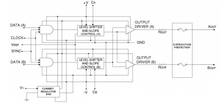
Functional Description: Modes: The BD429 operates in either a 429 mode or a 422 mode as controlled by the 429/422´ pin.
429 Mode: In 429 mode, the serial data is presented on the DATA(A) and DATA(B) inputs in the dual rail format defined in the MARK 33 Digital Information Transfer System – ARINC Specification 429-10. The driver is enabled by the SYNC and CLOCK inputs. The output voltage level is programmed by the VREF input and is normally tied to +5VDC along with V1 to produce output levels of +5 volts, 0 volts, and –5 volts on each output for ±10 volts differential outputs.
422 Mode: In 422 mode, the serial data is presented on DATA(A) input. The driver is enabled by the SYNC and CLOCK inputs. The outputs swings between 0 volts and +5 volts if VREF is at +5VDC.
Output Resistance: The driver output resistance is 75W ±20% at room temperature; 37.5W on each output. The outputs are also fused for failsafe protection against shorts to aircraft power. The output slew rate is controlled by external timing capacitors on CA and CB. Typical values are 75pF for 100 KHz data and 500pF for 12.5 KHz data.